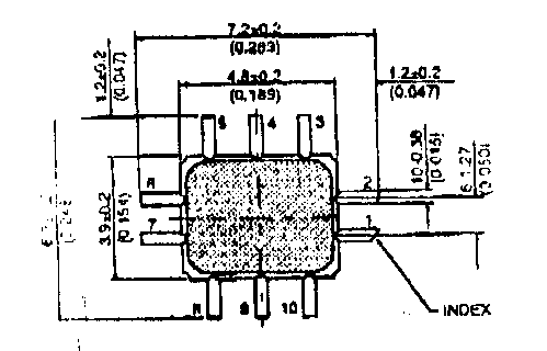
Milled Brass Carrier and PCB Assay.
(SMA connectors)

GaAs MMIC & PCB Installed

Bottom side of Brass Carried
with +5V regulator installed

Milled Brass Carrier and PCB Assay.
(SMA connectors)

GaAs MMIC & PCB Installed

Bottom side of Brass Carried
with +5V regulator installed
When soldering in the PCI3, the solder side should have ground area edges soldered to the brass carrier as well.
In my circuit, I use the +5V circuit and pin 8 output is not used, it but is connected to the +5V as shown. Each 50 ohm resistors is made up of 2 X 100 ohm 1% chip resistors.
These devices are available from Fujitsu USA at a cost of $37.00 US funds each. Fujitsu has a minimum billing of $ 200.OO US. This can easily be overcome by getting together with others to increase quantity ordered. The performance of the device in my system is nearly identical to the specs from the sheet that is provided with the device and the counter works very, very well.
When soldering the MMIC onto the PCB, first place a touch of solder to the belly (underside) of the device, align carefully and apply enough heat to the ground area near the device to melt the solder on the device.
This provides better heat sinking for the device than simply just using
thermal compound.
If anyone has a question that I might be able to answer, I can be contacted via:
Phone: 1 506 738-2734
FAX: 1 506 734-8512
E-mail: Darrell
Schematic for FMM110VJ Pre-Scalar
(0.0471
Positive Supply Voltage
VDD= +5V Operation Circuit


For further Information please contact:
FUJITSU COMPOUND SEMICONDUCTOR, INC.
2355 Zanker Fid.
San Jose, CA 95131-1138, U.S.A.
Phone: (408) 232-9500
FAX: (408) 428-91 11